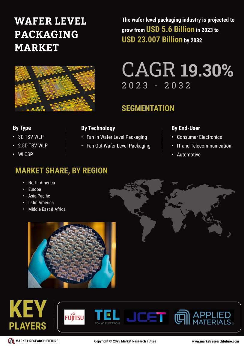
Wafer Level Packaging (WLP) has emerged as a transformative technology in the semiconductor industry, offering significant advantages in miniaturization and performance. This innovative packaging method encapsulates semiconductor devices at the wafer level, enabling a more efficient and cost-effective production process. The Wafer Level Packaging market is witnessing rapid growth, driven by the increasing demand for compact and efficient electronic devices.
WLP has revolutionized how semiconductor devices are packaged and integrated into various applications. Unlike traditional packaging techniques that require individual die to be packaged separately, WLP allows for the packaging of multiple dies on a single wafer. This not only reduces the overall footprint of the device but also improves performance by minimizing the distance between the chip and the package. As a result, WLP has become a preferred choice for manufacturers aiming to meet the demands of modern electronics.
The growing trend towards miniaturization in consumer electronics, telecommunications, and automotive applications is a primary driver of the WLP market. As devices become smaller and more powerful, the need for efficient packaging solutions that can handle increased functionality without compromising performance is crucial. WLP addresses these needs by providing a compact form factor that enhances thermal and electrical performance.
@https://www.marketresearchfuture.com/reports/wafer-level-packaging-market-12295
Wafer Level Packaging (WLP) has emerged as a transformative technology in the semiconductor industry, offering significant advantages in miniaturization and performance. This innovative packaging method encapsulates semiconductor devices at the wafer level, enabling a more efficient and cost-effective production process. The Wafer Level Packaging market is witnessing rapid growth, driven by the increasing demand for compact and efficient electronic devices.
WLP has revolutionized how semiconductor devices are packaged and integrated into various applications. Unlike traditional packaging techniques that require individual die to be packaged separately, WLP allows for the packaging of multiple dies on a single wafer. This not only reduces the overall footprint of the device but also improves performance by minimizing the distance between the chip and the package. As a result, WLP has become a preferred choice for manufacturers aiming to meet the demands of modern electronics.
The growing trend towards miniaturization in consumer electronics, telecommunications, and automotive applications is a primary driver of the WLP market. As devices become smaller and more powerful, the need for efficient packaging solutions that can handle increased functionality without compromising performance is crucial. WLP addresses these needs by providing a compact form factor that enhances thermal and electrical performance.
@https://www.marketresearchfuture.com/reports/wafer-level-packaging-market-12295
0 Commentaires
0 Parts
281 Vue
0 Aperçu